Application potential of graphene in microelectronic devices
- 2022-05-26
Since graphene was first mechanically exfoliated in 2004, it has quickly become a research hotspot in materials science, thanks to the fact that it can be used to do incredible things. The following articles will focus on how it will revolutionize semiconductor engineering in the years to come.
Graphene monolayers are composed of single-atom-thick carbon deposits. Because the nuclear bonds hold these atoms together, the resulting structures have extraordinary strength. The material's robustness means it can perform in the most challenging operating environments (handling high temperatures and large breakdown voltages). In addition to this, graphene offers a higher level of electron mobility (more than 130 times greater than that of silicon), which translates into extremely attractive conductive properties.
The Value of Graphene in Various Branches of Electronic Engineering
There are several key areas in microelectronics that could benefit from the use of graphene. These include:
Power systems - Complementing wide bandgap semiconductor technologies (i.e. silicon carbide and gallium nitride), graphene will be able to break through some of the bottlenecks in this field, which will lead to faster switching and significantly improved efficiency.
Optoelectronics - Graphene's high optical transparency means that it can be used in displays (providing an alternative to the indium tin oxide films currently used).
Data processing - Adding graphene to high-density microprocessor resources can greatly increase throughput. This will help to break through the "Moore's Law" that has long defined the semiconductor industry, and overcome the power leakage problems caused by the move to smaller process nodes.
There is also great market potential including Internet of Things (IoT) and other IoT devices.
Sensors present some very lucrative opportunities for graphene. Analyst firm Research & Markets estimates that the global graphene-based sensor business will be worth about $980 million a year by 2024. The main uses outlined in its recent report are in biosensors and optoelectronic devices. Especially when it comes to electronic sensors, graphene is thought to have the properties needed to function in the near future. However, the success of this material in these fields depends to a large extent on having an efficient production method.
By obtaining exfoliated graphene flakes, certain microelectronic devices can be produced in small batches. However, by its very nature, the global microelectronics industry does not work that way. This is all because of economies of scale, with large numbers of devices being manufactured at lower unit costs. If graphene is to be successfully incorporated into a new type of microelectronic device, the process used to synthesize graphene must be exactly the same as that used for semiconductor fabrication.
Synthesis of Graphene for High Yield Demand
The main methods currently used for large-area graphene synthesis are chemical vapor deposition (CVD) and plasma-enhanced chemical vapor deposition (PECVD). It must be noted that both processes have significant problems associated with them.
When producing graphene using the CVD/PECVD method, the synthesis is carried out on a metal catalyst (usually copper or nickel foil) rather than on the actual semiconductor substrate. The synthesized graphene must be removed from the metal foil and transferred to the semiconductor substrate. Therefore, it is very difficult to ensure the purity and structural integrity of graphene produced by these methods. The presence of pollutants poses a real threat. This could be the metal foil left over after the chemicals used in the transfer process or the catalyst has corroded. These contaminants or structural anomalies can adversely affect the performance parameters of synthesized graphene.
The metal-organic chemical vapor deposition (MOCVD) process developed by Paragraf means that CVD and PECVD are no longer the way forward for graphene synthesis. This patented process is truly unique because it enables the mass production of graphene and other two-dimensional (2D) materials. Unlike the CVD/PECVD arrangements already discussed, which require transfer from the pristine catalyst, MOCVD allows the direct layering of graphene materials onto semiconductor substrates. Inconvenient transfer steps can be avoided, so contamination is no longer considered a problem.
Graphene can be placed directly on full-scale semiconductor wafers in a consistent and fully repeatable manner. This means idm and fabs will be able to incorporate the MOCVD process into their already established workflows without any disruption.
Graphene-Based Magnetic Sensor Devices
One of the early openings for graphene was in the Hall-effect sensor market. Widely used in industrial and automotive systems, these sensors provide a non-contact mechanism by which the flux density of a magnetic field can be determined.
Conventional Hall effect devices have a three-dimensional (3D) sensing element, where the height of the element affects the results obtained. Magnetic field components that are not perpendicular to the direction of the sensing element may have an effect on the detected magnetic field strength, giving a false number. This phenomenon is called the "planar Hall effect".
Distinguishing between true and false signals means that additional components need to be included in the signal conditioning circuit (and thus increase the bill of materials). Otherwise, mathematical models may need to be built, although this is not suitable for situations that require real-time measurement data (such as vehicle safety systems, etc.). Other disadvantages associated with traditional Hall-effect sensors include that dynamic range and accuracy are affected by temperature variations.
Since graphene is a two-dimensional material, it has a major advantage in accurately measuring magnetic fields, as the thickness of the sensing element does not need to be considered. Hall-effect sensors that use graphene monolayers instead of traditional sensor elements will be able to support higher accuracy, as any errors caused by the planar Hall effect can be eliminated. Other advantages to consider include the higher thermal stability of graphene, which means that any device using graphene as a sensing element is immune to errors caused by temperature fluctuations. This will allow these devices to be deployed in extreme temperature applications.
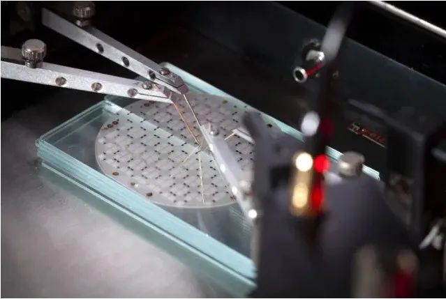
Electrical parameters of Hall-effect sensor die tested on wafer
Graphene-based Hall-effect sensors have also been seen before, but these sensors can only be produced in small batches with large unit costs, failing to achieve the necessary economies of scale discussed earlier. Thanks to the MOCVD process, Paragraph's GHS series of sensors can produce the volumes expected by industrial and automotive customers. These devices are not affected by the planar Hall effect because they rely on graphene monolayers. Therefore, they provide greater accuracy when determining the strength of the magnetic field. They provide nT resolution levels without requiring additional signal conditioning hardware. Therefore, the sensor system is more linear. In addition, they have a larger dynamic range compared to conventional Hall-effect sensors, while also improving temperature stability and superior linearity.
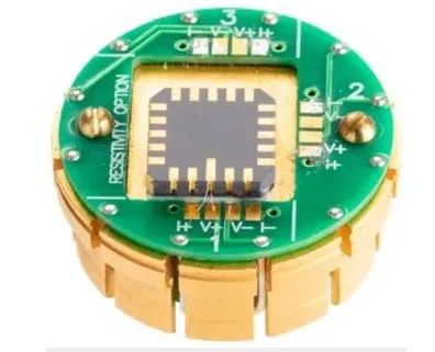
Example of a Paragraf GHS Hall Effect Sensor - the first in a series of advanced graphene-based devices developed by Paragraf
By leveraging a game-changing synthesis process, graphene (and the many operational advantages that come with it) can finally be used in commercially produced microelectronic devices. Electronic component manufacturers can now obtain large-area graphene through Paragraf without being hindered by contamination issues. While there have been many attempts to make graphene viable in a microelectronics environment in the past, this is the first time it has actually been achieved in a way that meets the high-volume production requirements required by the industry.
